
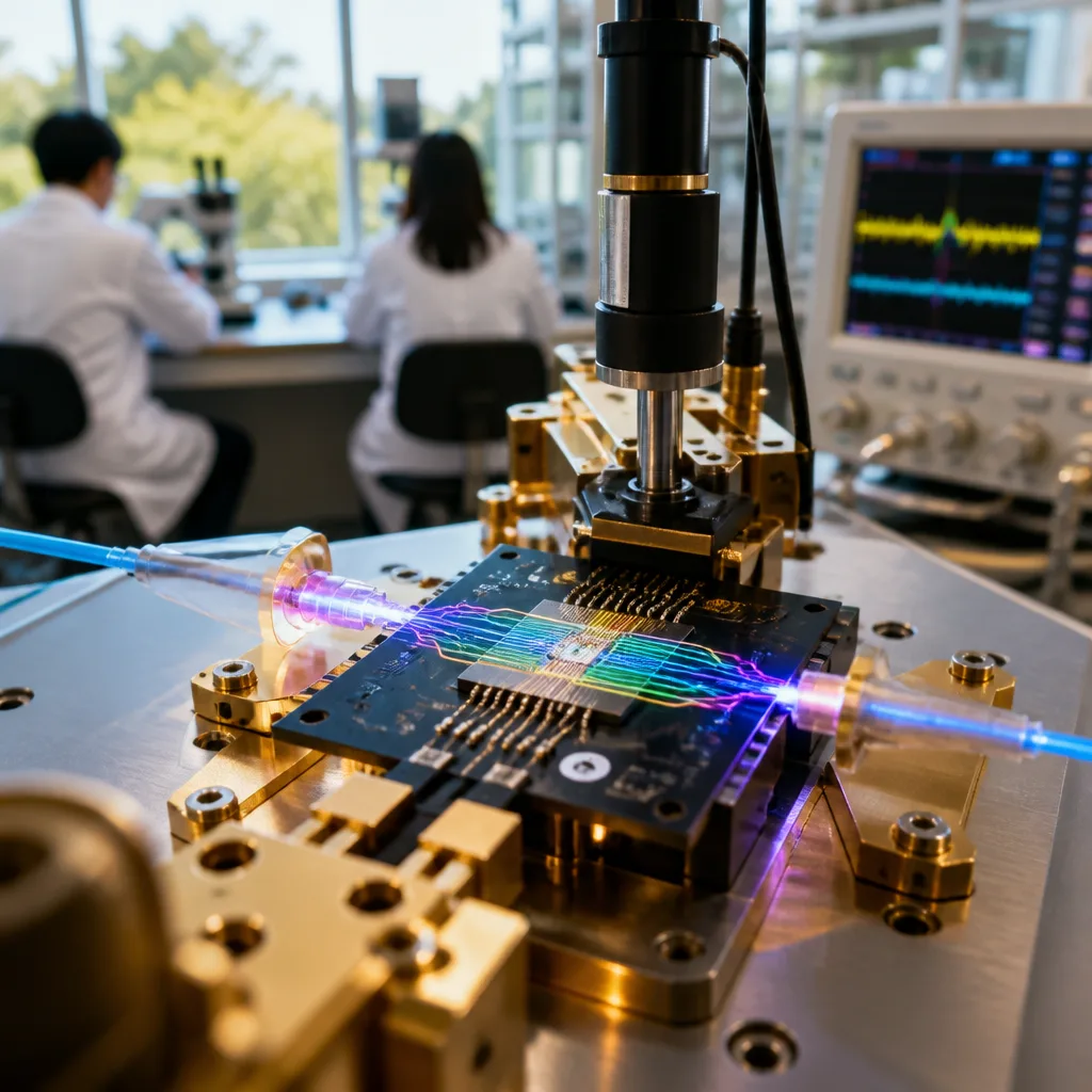
A group of engineers in South Korea has developed a programmable photonic integrated circuit that can deliberately slow, delay and shape pulses of light on a single chip — a capability that could help overcome a key barrier to optical computing and faster, more energy‑efficient data networks.
Why slowing light matters
Light carries data at extremely high speeds, but that very speed can be a liability when systems need to hold, delay or synchronise optical signals. Electronic systems rely on well‑established memory and buffering. Optical processors, which promise higher bandwidth and lower power use for tasks such as large‑scale artificial intelligence, have struggled to recreate equivalent functions in the optical domain.
Researchers led by Professors Namkyoo Park and Sunkyu Yu from the Department of Electrical and Computer Engineering at Seoul National University, together with Professor Xianji Piao of the University of Seoul, say their design gives engineers programmable control over both the speed and the temporal profile of light pulses inside a compact photonic chip. Their findings appear in the journal Advanced Science.
How the device works
The device exploits controllable interactions between optical resonators on an integrated circuit. By adjusting coupling among resonant elements, the chip can change how long an optical pulse spends inside the circuit and can also alter its frequency characteristics. The research team describes the architecture as a programmable circuit employing a coherent resonator‑induced transparency (CRIT) approach that permits flexible, on‑chip manipulation of so‑called "slow light."
- Programmability: Coupling between resonators is adjustable to tune delay and pulse shape.
- Integration: Functionality is implemented on a single photonic integrated circuit rather than relying on bulky external components.
- Applications: Potential for low‑power optical computing, buffering in AI servers and improved optical communications.
The researchers note their approach provides finer control than earlier proposals for slowing light, which were often limited in either the magnitude of delay or the extent to which pulse properties could be preserved.
Potential impact and limitations
If the technique scales and integrates with existing manufacturing processes, it could contribute to energy savings in data centres and accelerate development of optical processors that handle the surging workloads of generative AI and other large‑scale models. Optical computing promises advantages in bandwidth and energy efficiency, but practical progress has been hindered by the lack of compact, reliable optical memory and buffering.
By offering an on‑chip method to delay and reshape optical signals, the CRIT photonic circuit addresses a core architectural need: timing and synchronization in all‑optical systems. That capability could reduce reliance on electronic conversions and their associated power and latency penalties.
However, publication in a peer‑reviewed journal does not guarantee immediate commercialisation. The engineers will need to demonstrate the design in practical system settings, show compatibility with photonic manufacturing flows and quantify tradeoffs such as insertion loss, bandwidth limits and thermal sensitivity. The research report focuses on the circuit design and experimental demonstrations; broader system integration remains an active engineering challenge.
| Lead researchers | Institution |
|---|---|
| Namkyoo Park | Seoul National University, Department of Electrical and Computer Engineering |
| Sunkyu Yu | Seoul National University, Department of Electrical and Computer Engineering |
| Xianji Piao | University of Seoul, School of Electrical and Computer Engineering |
The work adds to a growing international effort to move more information processing into the optical domain. For countries and companies weighing investments in AI infrastructure, optical chips that reduce power consumption while preserving or improving latency could become strategically important.
For now, the results mark a step forward in photonic circuit design: a programmable element that can tune how light propagates in time and frequency on a compact platform. Whether it becomes a cornerstone of next‑generation AI servers or high‑speed networks will depend on subsequent demonstrations of reliability, manufacturability and system‑level benefits.
Reporting for NEXO RADAR's science desk.